

Introduction
Since cadmium zinc telluride (CZT) has several advantages including a high detection efficiency, good energy resolution and operability at room temperature without cooling device, it is a promising material for gamma-ray detection [1]. However, the weighting potential of a CZT detector with planar electrode is linearly distributed with its depth and it means that the amplitude of induced signals depends on the interaction position [2]. The incomplete charge collection due to trapping also occurs, because of low mobility and short lifetime of its hole. Therefore, in general, a detector applying a small pixel structure, coplanar grid and virtual Frisch-grid have been developed instead of the planar electrode [3ŌĆō5].
Among them, the Polaris-H (H3D Inc., Ann Arbor, MI, USA) and the Rena-Mini long (Kromek, Durham, UK) were typical commercialized products. They showed good spectroscopic performances and were able to reconstruct Compton images by using three-dimensional (3D) position and energy information [6]. However, due to the structure based on a large single crystal, there is a limitation that the cost dramatically increased as increase of the crystal size. To overcome this problem, an array type detector which was comprised of individual virtual Frisch-grid CZTs was proposed [7ŌĆō9]. Those small but high yielding components make the total price lower than that of monolithic detectors. The array structure also has the advantages in the achievement of large effective area by adding the elements and the maintenance of the detector performance by replacing the faulty parts.
In this study, we fabricated a prototype of CZT array detection system which consisted of virtual Frisch-grid CZTs, a detector holder, anode/cathode boards and an application specific integrated circuit (ASIC). Redlen CZT crystals (Redlen Technologies, Saanichton, Canada) and a Rena-Mini short with embedded RENA-3 ASIC (Kromek) were used [10, 11]. The detector holder and boards were designed to be compatible with them. The energy spectra were acquired to evaluate the performance. In addition, to verify the feasibility as radiation monitoring device for laboratories, nuclear power plants in decommissioning, etc., the weighted list-mode maximum likelihood expectation maximization (MLEM) method was applied to the output data and the Compton images were obtained. In case of the imaging, simulations were also carried out to understand the results. The all experiments and simulations were conducted using a 137Cs point source.
Materials and Methods
1. Array Module
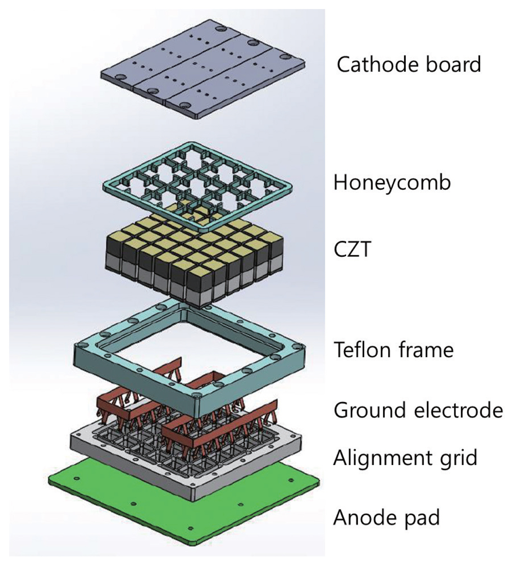
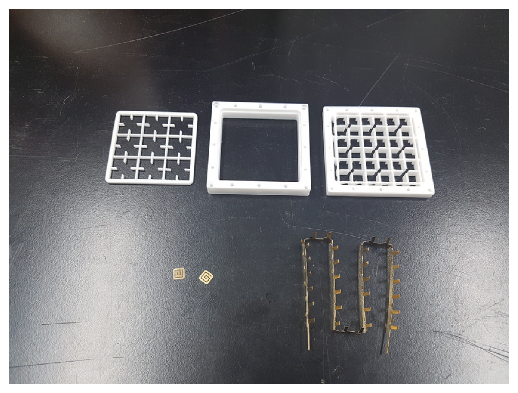
Fig. 1 shows the schematic of the array module. The prototype was designed based on a 6├Ś6 array of the 5├Ś5├Ś12 mm3 CZTs and its pixel pitch was determined to be 7.1 mm considering the CZT size and a fabricable septal thickness of the holder. Fig. 2 shows the manufactured holder and special electrodes. The detector holder which was made of Teflon, an insulating material, consisted of a honeycomb, a frame, an alignment grid for arranging the CZT detectors. The thicknesses of each part were 0.5 mm, 7 mm, 5 mm, respectively, and because the honeycomb was combined into a groove of the frame, the total thickness was same as that of the CZT. Spring type and ground electrodes were also fabricated by using 0.1-mm-thick beryllium copper (CuBe). The former were attached to the anode and cathode surfaces of CZT detector by using conductive epoxy for good contacts with the detector boards and sufficient resistance to external shocks. The latter was inserted between the frame and alignment grid to apply the voltage to a shielding electrode of virtual Frisch-grid CZTs.
2. Data Acquisition System
Fig. 3 shows the Rena-Mini short with dimensions of 46 mm├Ś80 mm├Ś98 mm. The device could be powered by a USB cable and provide the detector boards with high voltage up to 2,000 V. There were two built-in ASIC chips which had 36 independent channels for data processing. Since each channel has two signal paths, one with a fast shaper filter for timing and the other with a slow shaper filter for energy measurement, the both information could be measured, simultaneously. Moreover, the detail options as presented in Table 1 could be easily set via its software according to input signals and a type of detector. The input was digitized by a comparator with 8-bit threshold digital-analog converter and the output was transferred to PC. Power consumption was 6 mW or less per channel and a tolerance for the direct current (DC) leakage current was up to 5 nA.
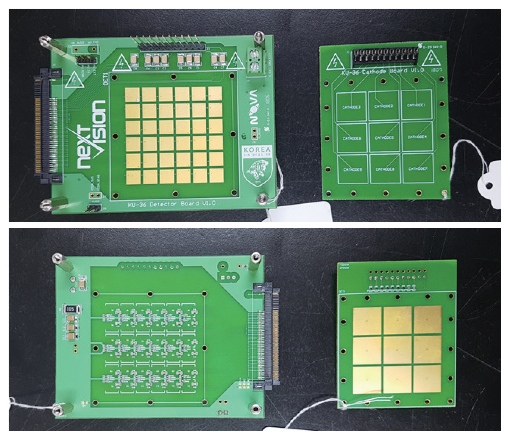
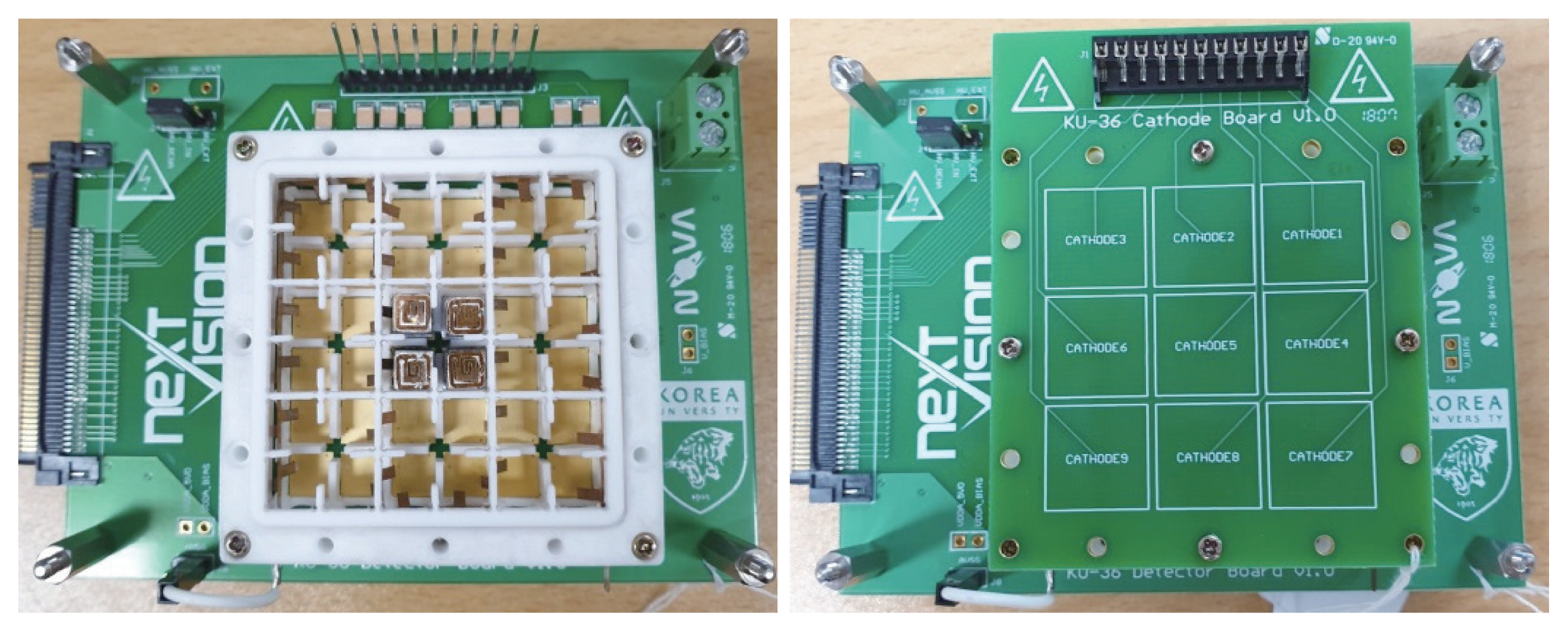
The detector boards were customized by Nova R&D, a subsidiary of Kromek, taking into account low electric noise, maximum applied voltage and resistance of the CZT (cf. Fig. 4). The electrodes on the anode board consisted of 36 while those on the cathode board formed a common electrode per 2├Ś 2 CZT array to reduce the necessary number of the channels. Every electrode was completely separated to minimize the crosstalk and the alternating current (AC) coupling was applied for protecting the circuit from the DC current.
3. Virtual Frisch-Grid CZT
The non-contacting shielding electrode method was applied for the virtual Frisch-grid effect [9] and the specifications of the used Redlen CZT are presented in Table 2. First of all, the side surfaces of each detector were wrapped by an ultra-thin polyethylene terephthalate hot shrink tube which has a dielectric strength over 150 V/╬╝m. Then, 1/3 of them closet to anode were covered with an aluminum tape to form the shielding electrode. Fig. 5 shows CZT detector before and after applying the virtual Frisch-grid method.
In general CZT detectors, the depth of the interaction can be inferred by the electron cloud drift time which indicates the time difference between the signals from the cathode and the anode. Since it was possible to measure the timing information of the both electrodes in current system, the 3D position sensing could be achieved by combining the acquired depth and the position information from the responded pixel. In this study, the spatial resolution determined by the pixel size was 5 mm in the x, y-direction and that in z-direction was 0.75 mm, because each detector was virtually divided into 20 bins along the depth. The 3D position was used to correct the position dependency of the signal amplitude and reconstruct the Compton images.
4. Image Reconstruction
When Compton scattering and photoelectric absorption sequentially occur, the incident direction of the gamma-ray can be reconstructed via Compton imaging technique. For Compton imaging, a scattering angle and an axis of each event are required. The scattering angle ╬Ė is calculated by the measured energy as follows:
where E0 is the incident energy, E1 is the energy deposited in the first interaction, me is the electron mass, and c is the speed of light. The axis is defined by extrapolating from the second to the first interaction position. Then, a cone based on the scattering angle, the axis, the location of the first interaction can be back-projected on the source plane as shown in Fig. 6. After repeating the back-projections of many events, the overlap of the cones indicates the source position.
To make the source distribution more precise, the weighted list-mode MLEM [12], iterative method based on the statistical model, was applied as described in Equation (2).
where ╬╗jn and ╬╗jn+1 are the current and new estimates, respectively, of the pixel j in the source plane for the n-th iteration, N is the number of detected events and Yi is the measured number of counts as event i. The event i was defined by information of the scatter detector element, the absorption detector element, and the scattering energy [13]. cij, called the system matrix, is the probability that a photon emitted at pixel j is detected as event i. It was calculated considering the probabilistic angular distribution of the Compton scattering, the distances between the interaction positions and the radiation attenuation in the detectors.
In weighted list-mode MLEM, theoretically calculated total angular uncertainty of event i, ╬ö╬Ėi was added to Yi as follows:
where
╬ö ╬Ė e n e r g y 2 , ╬ö ╬Ė g e o m e t r y 2 ╬ö ╬Ė D o p p l e r 2
5. Experiment Setup
The array module was assembled with four CZT detectors as shown in Fig. 7 and connected to the ASIC in an aluminum faraday box to block external electromagnetic fields. Fig. 8 shows the photographs and cross-section of the experiment setup. The 650 kBq 137Cs source was positioned 5 cm away from the center of the array and was measured at room temperature for 10 minutes. The anode and the shielding electrode were grounded, and the negative high voltage was applied to the cathode. Since a 100 V/mm or less bias was usually applied to prevent the electronic noise, the cathodeŌĆÖs bias was set at ŌłÆ1,200 V. The threshold and gain were chosen appropriately and the shaping time of the anode and the cathode were set to 1.1 ╬╝s and 2.3 ╬╝s, respectively.
Results and Discussion
1. Spectroscopy
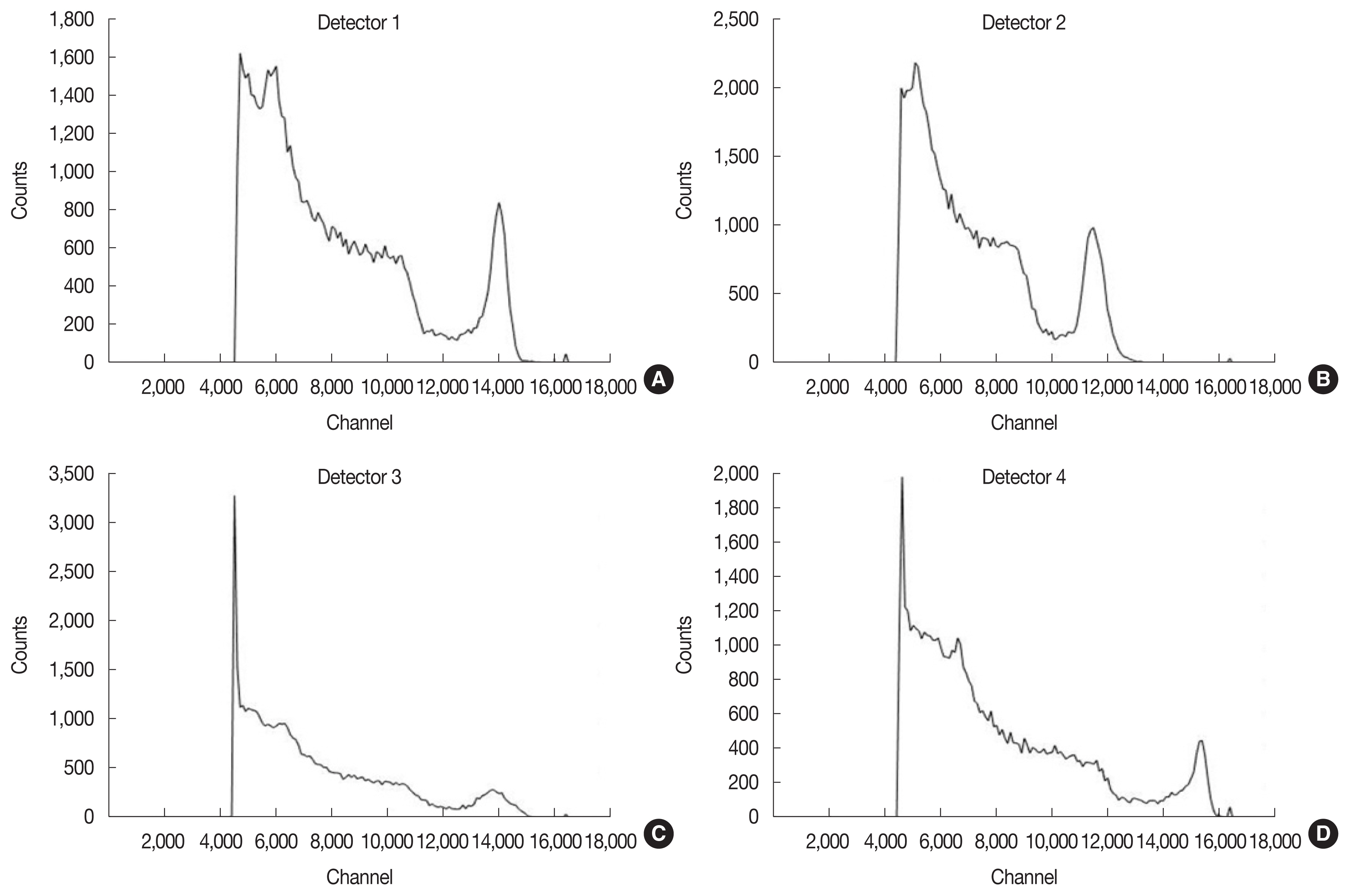
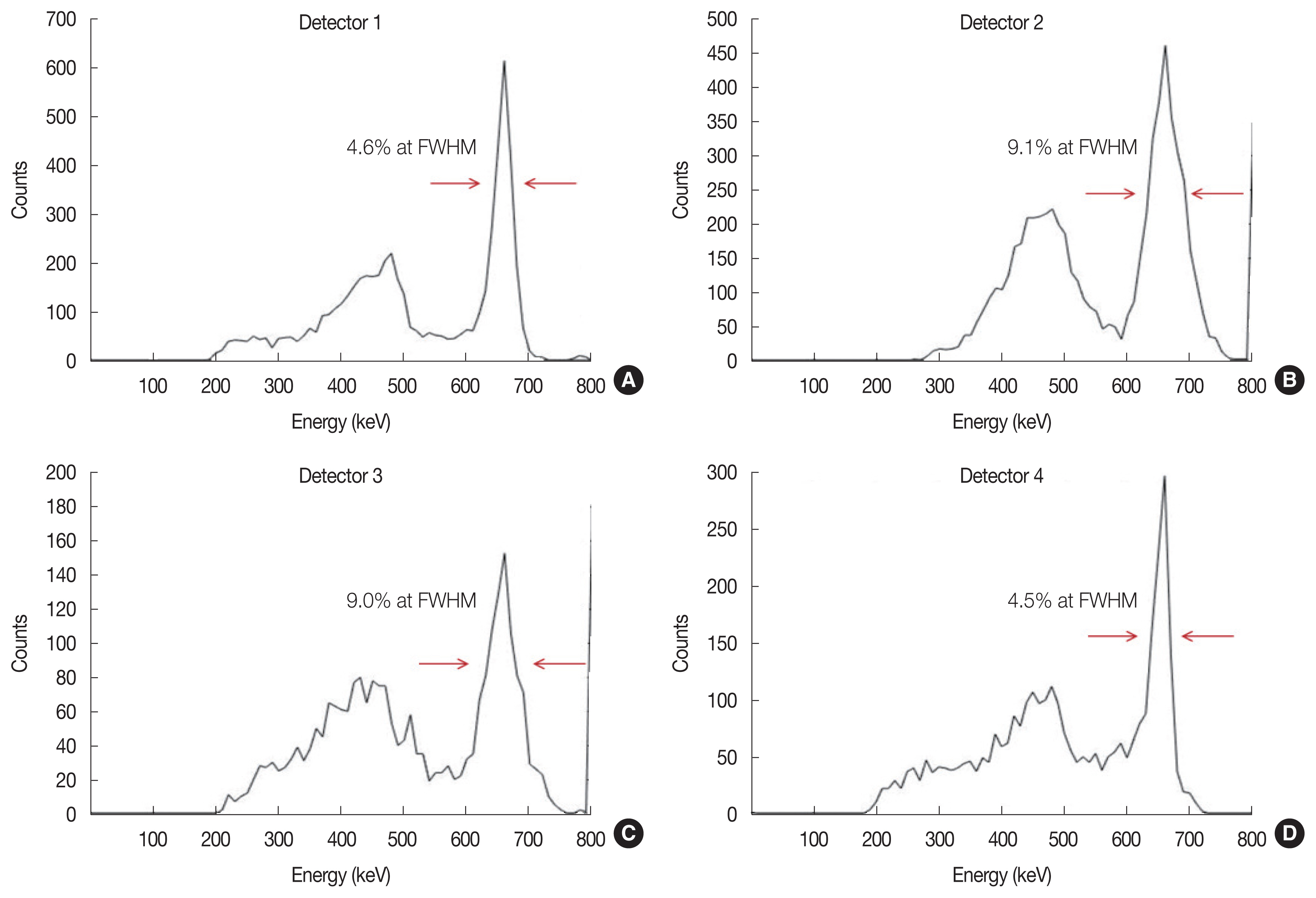
Fig. 9 represents the pulse height spectra of the triggered events on anode. Each CZT detector showed different performances but represented a general shape of uncorrected spectrum. The energy resolutions before correction were 5.8%, 8.6%, 12.8%, and 6.5% at 662 keV, respectively. To applying correction method, we extracted the events that both electrodes were triggered at the same time and acquired the 3D position information. Then, the correction was applied by multiplying the signal amplitude with a correction factor corresponding to the position where the signal occurred. The factor was a ratio of the peak channel of the total spectrum to that of each voxel. After the correction, the overall results showed the improvements as shown in Fig. 10. The photopeaks became sharper and the peak-to-Compton ratio which was the height of the photopeak divided by the height of the Compton continuum in spectrum increased. The energy resolutions were 4.6%, 9.1%, 9.0%, and 4.5% which were improved by 20% on average. However, owing to the intrinsic quality difference of the CZT crystal and the insufficient correction attributed to short measurement time, there were still the differences between the detectors. In addition, the low energy region of each spectrum was suppressed. This is because that there was a 15 kHz ripple noise in the cathode output and therefore its threshold was set high to remove it. We guessed that this noise was due to an incomplete rectification and a stable external DC high voltage supplier became a solution.
2. Compton Imaging
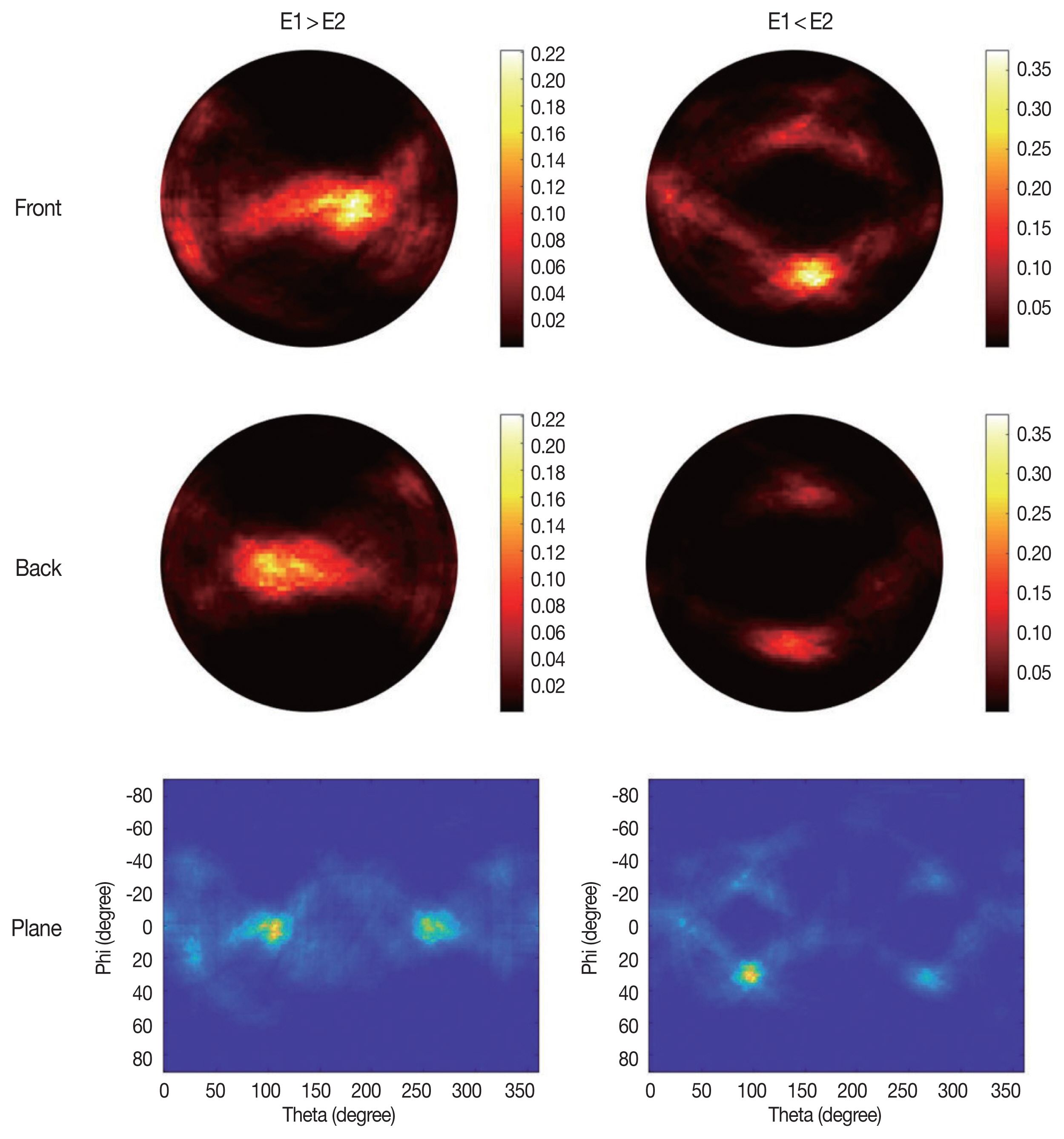
To determine the sequence order of Compton events, the simple comparison method based on the deposit energies of each interaction was used. Since the probability that a photon deposits more energy in the Compton scattering is affected by energy and an incident direction of the gamma-ray, a detector material and geometry, it depends on a detection system and situations. If the sequence orders of Compton events were wrong, they caused some artifacts on the opposite of source position or other sides on source plane. To determine the sequence order correctly, the simulations were preceded. The simulation tool was Geant4 Application for Tomographic Emission (GATE) v7.0. The detector structure was set up identically to the experiment and sources with 0┬░ŌĆō90┬░ offset were simulated. As a result, the ratio of deposit more energy in the Compton scattering was about 76% for all positions of sources, so we regarded the interaction delivering more energy as the first interaction [14].
Fig. 11 represents the planar Compton images of simulations based on the correct and opposite sequence orders and the number of iteration was 5. In case of the correct sequence order, each source was well located at its own position. However, because the measurable detection positions were very limited in the x and y directions, and the spatial resolutions of them were different from depth, the distributions showed the distortions according to increase offset angle. This angular dependency could be mitigated by adding the CZT components because the detectable position in x and y directions became various. In result of the wrong sequence order, the large artifacts appeared near the source and it makes the source difficult to distinguish. Fig. 12 shows the reconstructed 4ŽĆ and planar images in the experiment. The configuration of detection system and source was same as that of the 90┬░ offset source simulation. Compared the simulations, the result was similar but the artifact was dominant due to lack of the effective events. Table 3 shows a quantitative evaluation of the current system and a comparison of the Polaris-H, the Rena-Mini long, and a virtual Frisch-grid detector array from Brookhaven National Laboratory. This result represented that the current system needed to be developed, and if the entire system is completed, it is expected to be competitive with other systems.
Conclusion
In this study, the virtual Frisch-grid CZT detector based on 2├Ś2 array structure was developed and the experiment of 137Cs was performed. The energy and timing information of both the anode and cathode was acquired at the same time. Since it is possible to detect 3D position by calculating the drift time, the variations of signal amplitude were corrected in accordance with the interaction position. As a result, the energy spectra were improved but the low energy regions were not formed properly. This is because that the threshold of the cathode to eliminate the rippling noise was too high. To resolve this problem, the stable external DC high voltage supplied will be used in the future.
To identify the viability as a Compton imager, the weighted list-mode MLEM was applied to the output data. The simulations with various offset source were also performed and the sequence orders of the effective Compton events were determined by the deposit energies. In simulation results, the sources were well located at each offset angle but the performance was degraded with increasing of the offset angle due to the different spatial resolution x, y direction and depth. The Compton image of the experiment was successfully acquired and similar to that of the simulation.